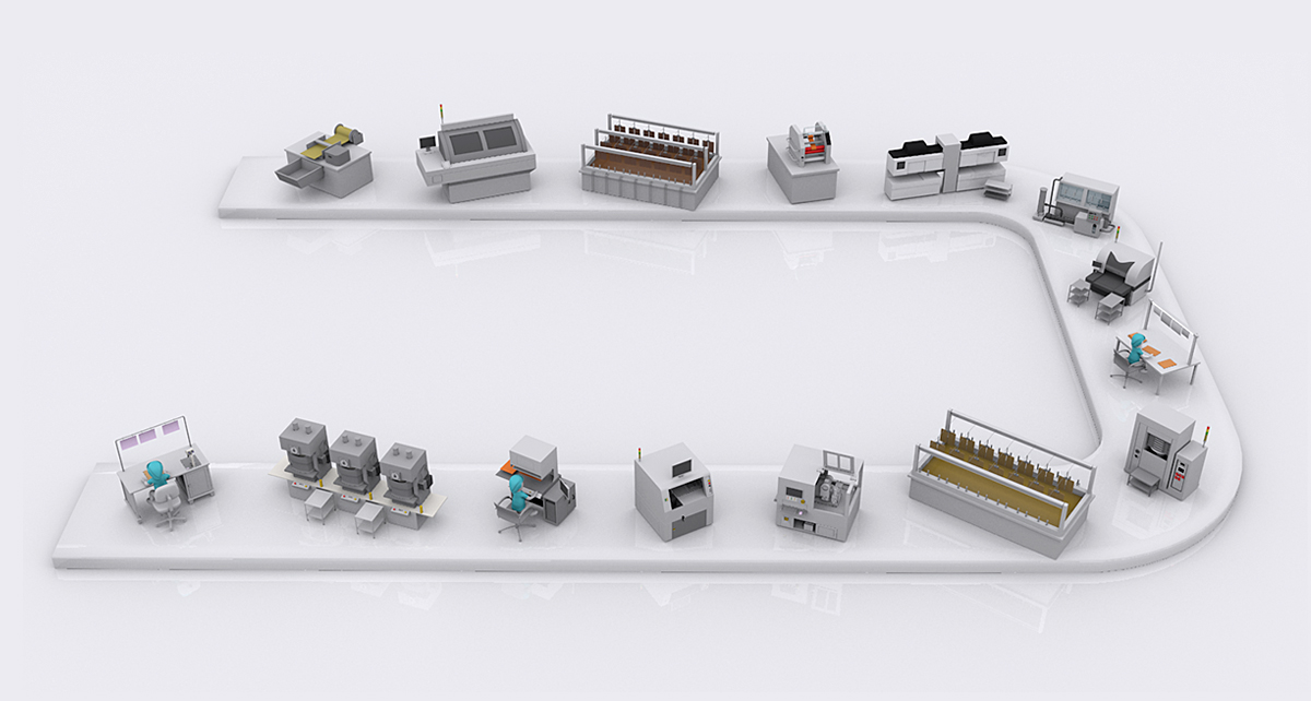
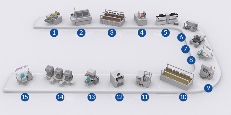
01Cutting process Process to cut raw materials (FCCL, Coverlay, Bonding Sheet, Prepreg, Copper foil) in rolled state into working size 02CNC process Process of processing through hole and laser via hole in base raw material for interlayer conduction 03Plating copper process The process of conducting chemical or electroplating to the non-conductive part of the processed hole (Through hole & Laser via hole) 04D / F adhesion process Process of adhering photosensitive film to form circuit on copper plated product 05Exposure process Process of irradiating UV on the adhered photosensitive film 06D.E.S process The process of forming a circuit by corroding copper by passing through a line consisting of development, corrosion and peeling 07AOI process The process of inspecting circuit sections after scanning with automatic optical inspection equipment 08Tack Welding process The process of melting cover-lay adhesive with an iron and attaching it temporarily with a base substrate 09Hot press process Process of thermocompression bonding at high temperature and high pressure to completely cure the welded product 10Plating surface process Process of plating the surface of copper foil exposed to cover-lay open section 11Automatic welding process Automatic welding: Process to attach reinforcing bars (Epoxy, Kapton, Sus) for reinforcement in FPCB flexible section 12Post-processing Process of processing guide hole for mold processing. 13BBT process Process to detect open and short between circuits using electrical characteristics 14Press process The process of processing the external appearance of the product through the press equipment and the mold. 15Inspection process The process of determining suitability for appearance and dimensions of the finished product through appearance processing.